


The Development Value and Application Advantages of Glass Core Substrates in the Era of Advanced Packaging
2026-05-29
As the semiconductor industry continues to evolve toward higher performance, higher density, and miniaturization, the traditional path of scaling down chip device dimensions to enhance computing power and performance—driven by Moore’s Law—is increasingly approaching physical limits and process bottlenecks. With transistor processes moving into 3nm, 2nm, and even more advanced nodes, scaling alone not only entails extremely high R&D and manufacturing costs but also introduces technical issues such as leakage current, uneven heat dissipation, and reduced stability, making it difficult to meet the extreme demands for comprehensive chip system performance in cutting-edge fields like artificial intelligence, high-performance computing, high-end servers, and high-speed communications. Against this industry backdrop, chip manufacturers are moving beyond traditional process iteration thinking and shifting their innovation focus to backend areas such as packaging and system integration. As a result, advanced packaging technology has emerged as a core innovation track to break through performance bottlenecks and sustain semiconductor industry upgrades.

As the central enabler of advanced packaging technology evolution, the material properties of the packaging substrate directly determine the interconnection precision, form factor, operational stability, and service life of chip packaging, making it a critical factor in the realization of high-end packaging solutions. Current mainstream packaging substrates are primarily based on materials such as resin and ceramics. While these mature materials are suitable for low- to mid-end packaging processes, their limitations become evident in ultra-large-scale, ultra-high-density high-end packaging scenarios. Common issues include low interconnection precision ceilings, relatively high coefficients of thermal expansion, insufficient dimensional stability, and severe warpage in large-scale processing—all of which fail to meet the development needs of high-end chips requiring multi-chip integration, high-density interconnects, and large-scale packaging.

To overcome the technical shortcomings of traditional substrate materials and align with the advancement of advanced packaging, glass core substrates have emerged as a next-generation high-end packaging solution being actively evaluated, developed, and deployed by the global semiconductor industry, leveraging their unique physical properties and process advantages. Compared with traditional substrate materials such as resin and ceramics, glass core substrates offer several disruptive advantages that holistically enable high-end packaging technology upgrades. First, their excellent structural characteristics support larger-scale integrated packaging, meeting the demands of multi-chip integration and high-compute module assembly, thereby significantly improving chip system integration and overall computing power. Second, the high surface flatness and excellent dielectric uniformity of glass materials enable finer and higher-density interconnect routing, effectively reducing line spacing, enhancing signal transmission efficiency, and minimizing loss and delay in high-speed signal transmission—perfectly suited for the performance requirements of high-speed computing and high-frequency communication chips. Finally, glass core substrates feature an extremely low coefficient of thermal expansion, providing exceptional dimensional stability. During high-temperature packaging processes and long-term operation under alternating high and low temperatures, they are less prone to deformation or warpage, thereby improving packaging yield and enhancing chip operational reliability and stability.

Currently, glass core substrate technology has entered the critical stage of process validation and small-batch testing. With continued industry investment in R&D and the ongoing maturation of manufacturing processes, the pace of large-scale adoption is expected to accelerate. Glass core substrates are poised to become a core material for future high-end advanced packaging, providing essential support for the semiconductor industry to overcome performance bottlenecks and achieve technological innovation and upgrades.
RELATED NEWS
-

SEMICON EUROPA 2026: Looking Forward to Meeting You in Munich
Europe's semiconductor industry is the leader in the industry and is indispensable. DOHONE is also continuing to provide stable supplies to European customers and continuously learning from them.
-

SEMICON Taiwan 2026: Looking Forward to Meeting You in Taiwan
As a manufacturer specializing in the production of semiconductor precision jigs and carriers, DOHONE has customers all over the world.
-
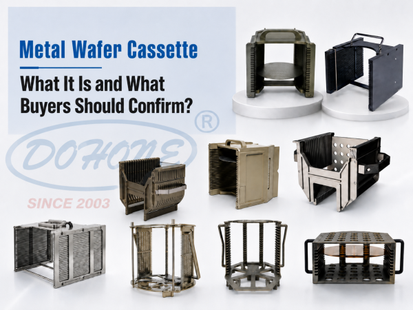
Metal Wafer Cassette: What It Is and What Buyers Should Confirm?
A metal wafer cassette is a precision carrier designed to securely hold, organize, and transport semiconductor wafers during high-temperature processing.
-
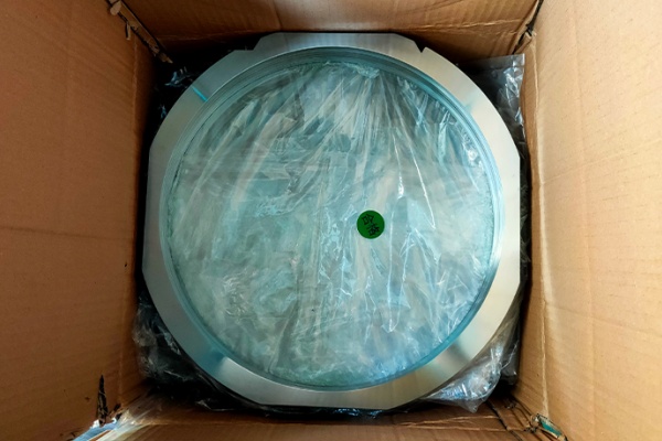
The hardness of DOHONE Wafer Dicing Rings reaches 50-55HRC, ensuring superior quality and reliability
When purchasing Wafer dicing ring, exquisite appearance and robust durability are core requirements.
-
How to Choose a High-Quality 6" High Temperature Cassette Manufacturer
The stable mass production of a high-performance chip relies on the quality support of the entire supply chain.
-
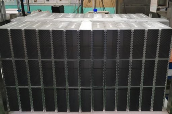
Customized Assembled Magazine Solutions for Semiconductor R&D and Testing
During the critical phase of new semiconductor chip development and prototype testing, small-batc.
-
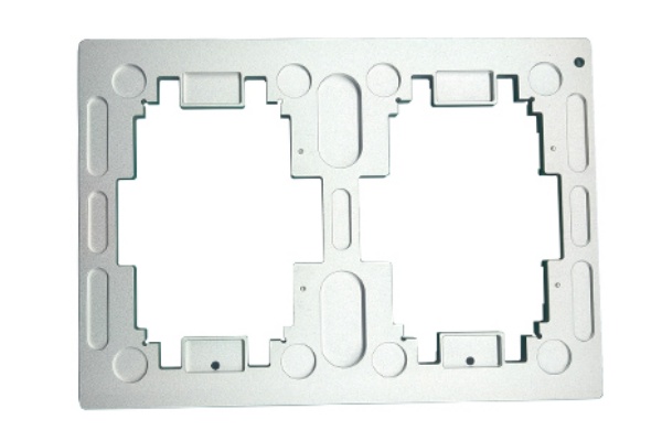
What should be noted when machining IGBT fixtures with CNC machine tools?
They are key equipment for defining the qualifications of precision machining companies and also the foundation for ensuring high-precision production.
-
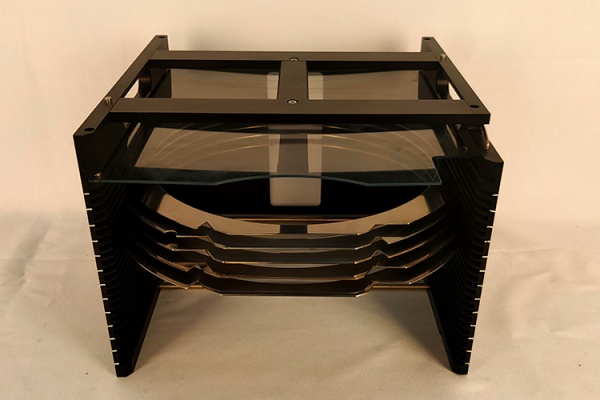
The Secret Behind Wafer Ring Cassette Manufacturers' Ability to Maintain High-Quality Products
In the processes of semiconductor wafer production, transfer, and storage, the Wafer Ring Cassette is responsible for carrying and protecting wafers.
-
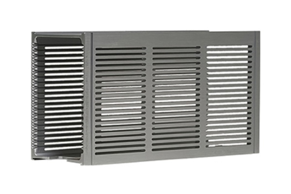
DOHONE's Solid Magazine is the "foundation" of the wire bonder
Semiconductor packaging and testing wire bonders rely on ultrasonic energy to bond gold wires and aluminum wires to chip pads and lead frames.
-
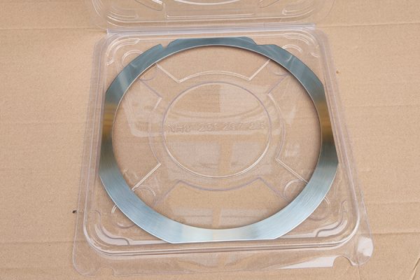
Which 8 Inch Wafer Frame Is Better?
High-quality 8 inch wafer frames depend on professional original manufacturers with strong R&D capabilities and mass production experience.
-
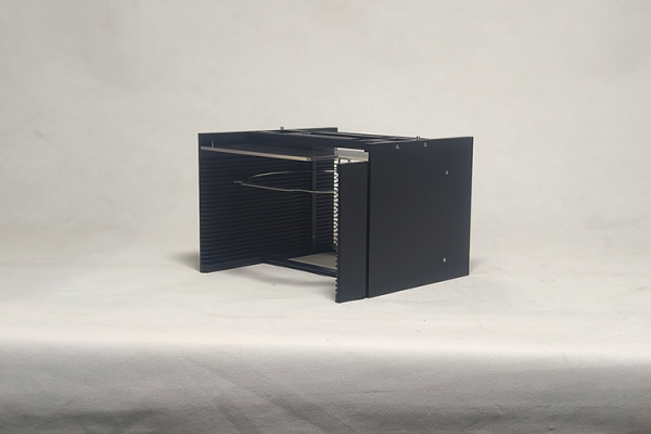
How To Screen A Wafer Cassette Manufacturer For Long-Term Cooperation
Many customers share a common procurement challenge when communicating with our sales team: although the number of wafer cassette manufacturers on the market continues to grow.
-
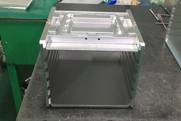
Eliminate quotation deviations—DOHONE's real-time quoting makes procurement more worry-free.
In the procurement process of semiconductor wafer carriers, the vast majority of customers share a common core concern: worrying that the quoted price for the wafer expanding ring cassette they receive is not a real-time price.
-

The Importance of Surface Quality for Precision Tray Fixture
The surface quality of precision Tray fixture is a core indicator for measuring product machining accuracy and overall performance.
-
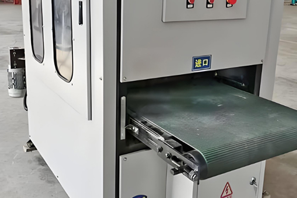
Surface Brushing Process Advantages for chip packaging material magazine
The surface brushing process on metal aluminum parts has long been widely recognized and adopted in the precision structural component, semiconductor carrier magazine.
-
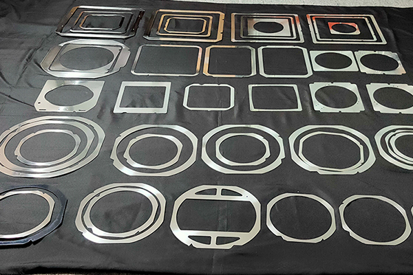
DOHONE 12-inch Metal Film Frame--Deep cultivation of quality drives repeat purchases
The core competitiveness of industry development has never been the mass production of conventional outputs, but rather the ultimate control over details.
-

Professional Manufacturer of Reflow Soldering Fixtures
Reflow soldering fixtures are indispensable tooling carriers in the field of electronic intelligent manufacturing, widely used in core processes such as SMT placement.
-
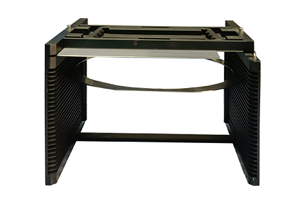
150mm Wafer Cassette Product Advantage Introduction
As semiconductor chip manufacturing processes continue to iterate and upgrade, the trends toward miniaturization and precision in chips have become increasingly prominent.
-
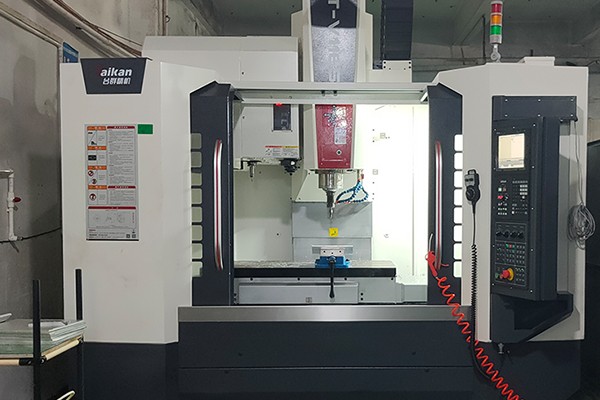
8" High Temperature Cassette Manufacturer "DOHONE" Better Understands Your Customization Needs
With the continuous rise in raw material, labor, and logistics costs, cost reduction and efficiency improvement have become the core objectives for semiconductor enterprises.
-

The wafer dicing frame continuously safeguards the wafer dicing process.
Semiconductor fabrication plants specializing in the wafer backend dicing process surely understand this well. As chips become more precise and miniaturized, the industry's standards for full-process wafer protection are continuously being upgraded.
-
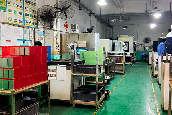
One-stop aluminum wafer cassette custom processing manufacturer – DOHONE Strength Introduction
Nowadays, comprehensive costs across various industries—including raw materials, labor, and communication management—continue to rise, putting increasing pressure on business production and operations.
-
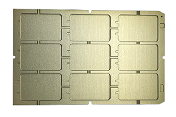
Analysis of Surface Quality in Welding Fixture Machining and Solutions
In welding fixture machining, many factors can affect the surface quality of the workpiece. In order to ensure that the surface quality of precision machined parts meets the roughness requirements.
-

We Prioritize Your Urgent Needs And Are Fully Committed To Resolving Your Wafer Film Ring Delivery Challenges!
Adhering to our service philosophy of putting customers' needs and concerns first, if you have bulk purchase requirements for Wafer film rings with tight delivery schedules and strict time requirements, DOHONE is your reliable and trustworthy partner.
-
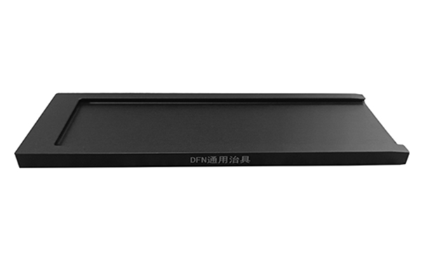
How To Choose A Jig Fixture Manufacturer?
In the semiconductor chip manufacturing industry, the machining precision and surface quality of components directly affect equipment operational stability and production quality.
-
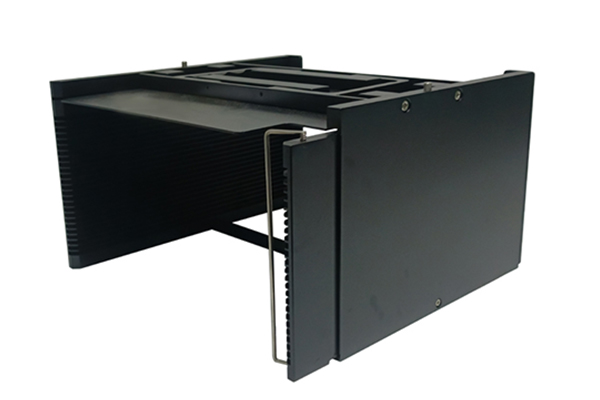
200mm Wafer Cassette Processing—Choosing The Right Manufacturer Is Crucial
As the semiconductor industry rapidly iterates and upgrades, core processes such as packaging, dicing, and scribing continue to become more refined and precise.
-
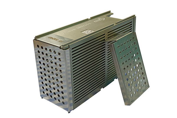
What Should Be Done About Stains On The Surface Of Ic Packaging Magazines
IC packaging magazines are the core carrying fixtures in semiconductor packaging and testing production lines.
-
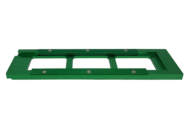
What Are The Types Of Precision Fixture And Jig Machining?
In the semiconductor chip production process, to ensure product quality and productivity, jigs and fixtures are commonly used as auxiliary tools.
-
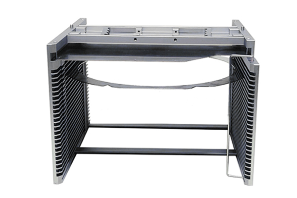
What Are The Reasons For Substandard Quality In Wafer Dicing Cassettes?
As an indispensable transport carrier in the semiconductor chip dicing process, the Wafer Dicing Cassette is primarily used to store and transport finished chips.
-

The Processing Workflow Of Semiconductor Fixture Manufacturer Products
When a semiconductor Fixture Manufacturer processes parts, it must not only meet the client's technical requirements for workpiece machining and achieve the required performance, but also focus on improving production efficiency and worker productivity.
-
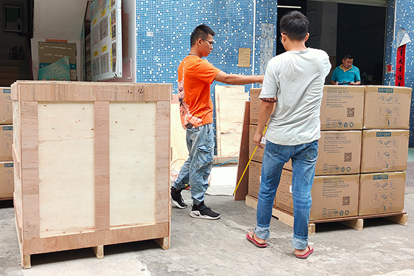
Aluminum Wafer Cassette Manufacturer "Dohone" – Standard Products Ship Within 48 Hours!
In the wafer dicing process, many aluminum wafer cassettes are used. Wafers of different specifications and sizes require corresponding wafer cassettes.
-
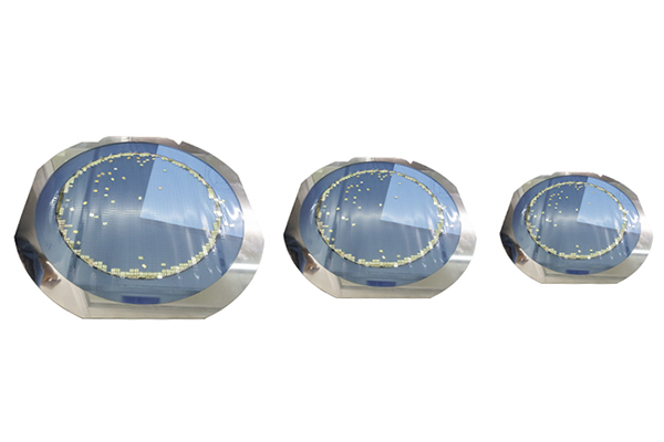
How Much Does A Semiconductor Wafer Frame Cost? - Inquire Now To Get A Free Sample.
How much does a semiconductor wafer frame cost? DOHONE helps you save money in 3 steps.
-
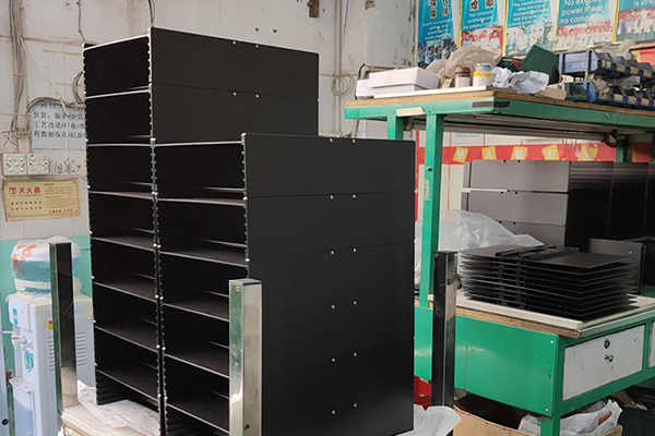
Which Manufacturer Can Customize 8 Inch Semiconductor Wafer Cassettes? - DOHONE
The semiconductor peripheral supporting field covers multiple industries. As the product iteration cycle in the semiconductor industry becomes shorter, companies need to continuously innovate and develop new products to meet market demands.
-
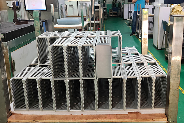
How DOHONE Meets Small-Batch Metal Slot Magazine Customization Requirements in a Rapidly Iterating Market
In today's ever-changing era, rapid shifts in market demand have become the norm. For the manufacturing industry, how to quickly respond to market changes and meet customers' customization needs has become the key to corporate competitiveness.
-
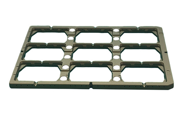
CNC Machining Center: The First Choice for Precision Tray Fixture Processing
Using CNC machines for precision tray fixture processing not only offers high production efficiency but also delivers good economic benefits.
-
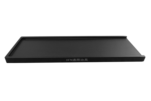
Which Precision Fixture machining factory is better?
In recent years, Precision Fixture factories have been emerging all over the world. For factories that require Precision Fixture machining, how to identify the quality of manufacturers and make the right choice among so many options has become a topic of concern.
-
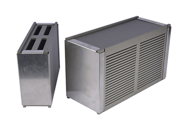
What Are the Factors Affecting the Machining Dimensional Accuracy of Riveted Magazines?
Riveted Magazines require extremely high precision during machining. If the machining accuracy is compromised, it will cause the product to mismatch with equipment data.
-
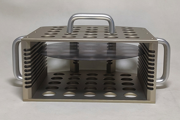
Small-Batch Metal Wafer Cassette Machining – Choose DOHONE for High Precision
In March of this year, a client from Malaysia, Mr. Lee, contacted DOHONE Company while searching online for a Metal Wafer Cassette machining supplier. His company had an aluminum alloy product that required small-batch custom machining.
-

Thin-Film Lithium Niobate (TFLN): The Core Benchmark Material for Next-Generation High-Speed Optical Switches and Optical Interconnects?
Thin-film lithium niobate is hailed as the "best alternative beyond silicon" in the field of photonics. With its ultra-high electro-optic modulation bandwidth, extremely low optical propagation loss, ultrafast response speed, excellent nonlinear optical properties.
-
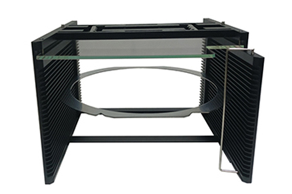
Choosing the right wafer frame cassette helps improve your die yield in the dicing process.
The chip manufacturing process is highly complex, involving everything from front-end steps such as photolithography, etching, and thin-film deposition to back-end steps like thinning, die dicing, and packaging/testing.
-

The Core Reason And Solution For Precision Fixture Machining Accuracy Failing To Meet Standards?
In the field of precision manufacturing, the machining accuracy of fixtures directly affects the quality stability of the final product. Many companies have encountered this situation.
-
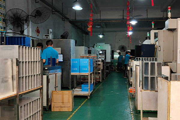
High-Quality Wafer Cassette: Core Supporting Guarantee for Semiconductor Chip Dicing and Production
As a core precision component for carrying, transferring, and storing wafers in the semiconductor chip manufacturing process, the quality of a Wafer Cassette is directly linked to wafer yield and the production efficiency of the entire line.
-
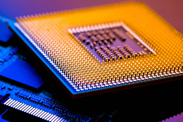
Global Semiconductor Industry Market Growth Trend Analysis for 2026?
From the end of 2025 to the beginning of 2026, the global semiconductor industry has entered a phase of cyclical prosperity.
-
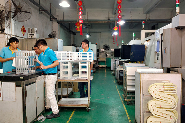
How DOHONE, a Precision Fixture Machining Factory, Strictly Controls Quality to Create High-Quality Products
It is often said that quality is the lifeblood of an enterprise, the core foundation for establishing a foothold in the market, and the fundamental confidence for the long-term development of the precision manufacturing industry.
-

Micron 256GB DDR5 RDIMM: Empowering Modern Data Centers to Overcome the Challenge of Surging Compute Demand
These emerging applications place unprecedented demands on the core performance of enterprise servers.
-

DOHONE Precision Fixture Processing
While striving to maintain its domestic trade, DOHONE has also been continuously developing overseas trade platform channels and opening up information promotion channels.
-
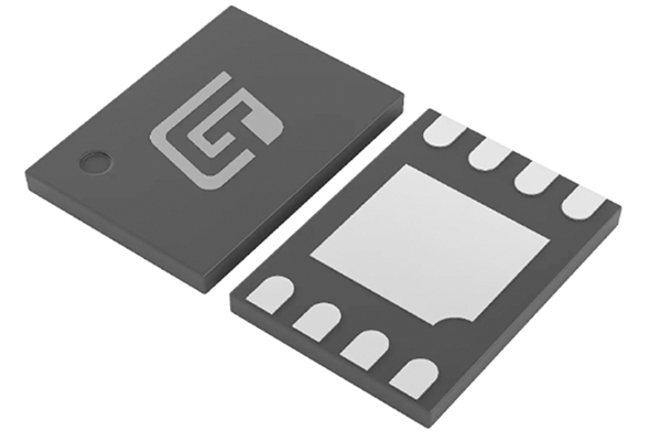
In Q1 2026, the global semiconductor market grew by 79.2% year-on-year
Driven by growing demand in data centers, AI applications, cloud computing, and automotive applications, the global semiconductor market grew by 79.2% year-on-year in the first quarter of 2026, with sales reaching $298.5 billion.
-
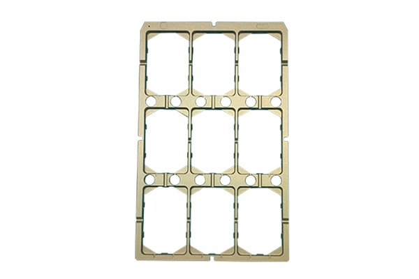
Classification of Precision Jigs
Jigs can be classified into three categories: process assembly jigs, project testing jigs, and circuit board testing jigs. Among them, process assembly jigs include assembly jigs, welding jigs, disassembly jigs, dispensing jigs, irradiation jigs, adjustment jigs, and cutting jigs.
-
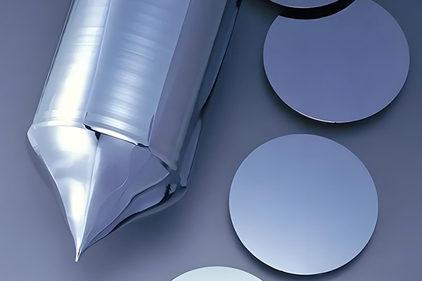
What is a silicon wafer?
What is a silicon wafer? In essence, it is a thin, circular slice of silicon that has undergone highly precision processing to achieve an extremely smooth surface.
-
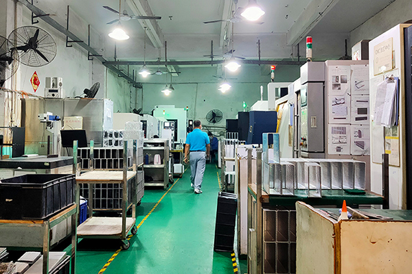
The Core and Importance of Precision in Semiconductor Fixtures
As a cornerstone of high-end manufacturing, the semiconductor industry is characterized by high technical barriers and complex production processes, demanding micron- or even nanometer-level precision at every step.
-

SK Hynix: Yield of HBM Hybrid Bonding Process Improved
SK Hynix has announced a significant yield improvement in its hybrid bonding process for High-Bandwidth Memory (HBM), according to the company’s technical leadership.
-
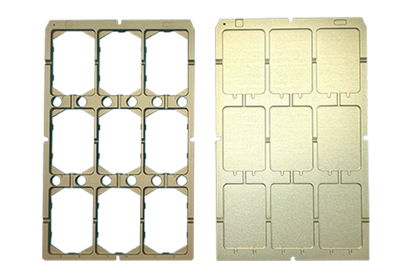
DOHONE Precision Jigs – Engineered from 7075 Aluminum for High-Frequency Production Lines
DOHONE precision jigs are manufactured entirely from high-strength 7075 aluminum alloy, a material widely recognized for its exceptional mechanical properties and fatigue resistance.
-
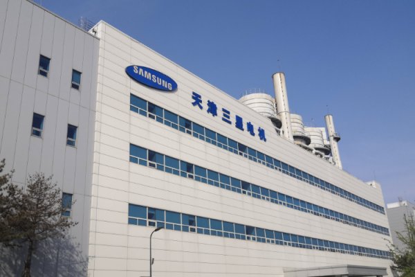
Samsung Electro-Mechanics Joins NVIDIA's Core Supply Chain, Supporting Mass Production of the Groq3 LPU Chip
Amid the rapid iteration of the global AI industry and the surging demand for AI inference, the supply chain landscape for core semiconductor components is being continuously reshaped.
-
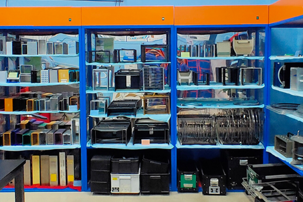
DOHONE Wafer Dicing Cassette: Empowering the Automation Upgrade of Semiconductor Packaging
As the global semiconductor industry rapidly iterates toward high precision, high integration, and miniaturization, chip manufacturing processes continue to break through to 3nm and below.
-
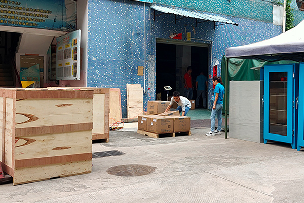
Choose the Right Wafer Frame Cassette to Avoid Fatal Hazards in Semiconductor Production – DOHONE Ensures Quality Protection
In semiconductor wafer processing, the Wafer Frame Cassette, as a core component for wafer storage, transport, and dicing, directly determines the stability, efficiency, and safety of production through its quality and precision.
-
The NAND Flash Supercycle Under the AI Wave: Soaring Prices and Structural Industry Transformation
The global semiconductor industry is currently experiencing a strong recovery, and the surge in NAND flash prices is undoubtedly the core engine and strongest driving force behind this rebound.
-
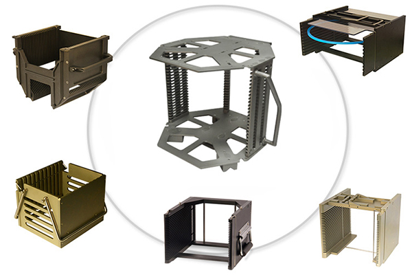
The "Universal Currency" and Intelligent Cornerstone of the AI World
In the AI era, why has memory become digital oil DOHONE empowers industrial breakthroughs with precision supporting solutions.
-
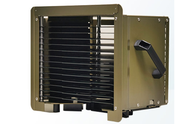
DOHONE Metal Wafer Cassette – Empowering High-End Semiconductor Chip Manufacturing
For many years, DOHONE has remained focused on the field of high-end semiconductor handling and carrier products, accumulating deep technical expertise and industry insight, particularly in the R&D and manufacturing of Metal Wafer Cassettes.
-
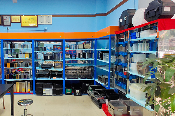
With the annual ISO quality system certification, DOHONE continues to strive for better product quality and service excellence
As an internationally recognized standard for quality management systems, ISO 9001 has long become the core foundation for the stable operation and quality control of large-scale enterprises.
-
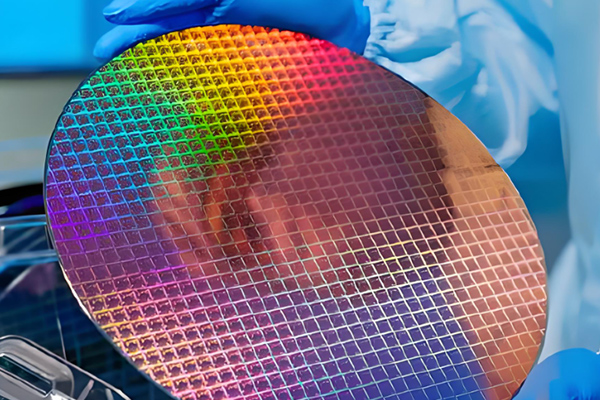
In 2026, The Global Wafer Foundry Industry Will Usher In A New Round Of Strong Growth
Entering 2026, the global wafer foundry industry will enter a new phase of robust growth, primarily driven by continued investment and intense competition in artificial intelligence from North American cloud service providers (CSPs) and AI startups.
-
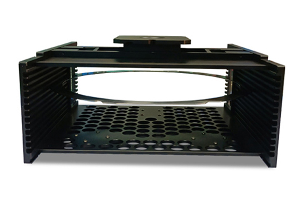
Wafer Frame Cassette Manufacturer – Committed to Serving Customers with Dedication
Many customers in the semiconductor industry have a clear criterion when looking for a Wafer Frame Cassette manufacturer.
-
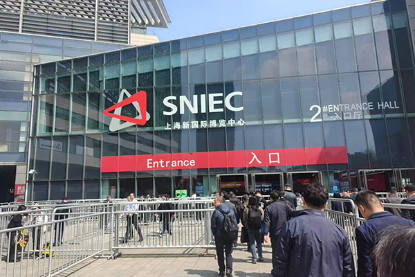
Semiconductor Industry Upgrades – DOHONE Continues to Focus on the Electronica China Exhibition
Currently, the global semiconductor industry is rapidly advancing toward higher precision, higher integration, and miniaturization.
-
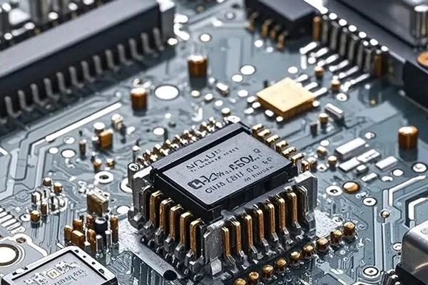
Global Semiconductor Industry Sales Increase 3.7% Month-on-Month in January
According to the latest reports from authoritative media, the global semiconductor industry experienced a "strong start" in January 2026, with monthly sales reaching $82.5 billion.
-
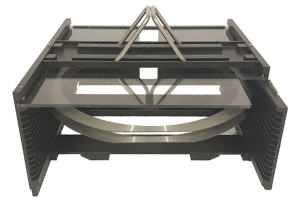
DOHONE Establishes In-depth Cooperation with Malaysian Agent
As the only country in the world that encompasses all industrial categories in the UN classification, China demonstrates significant competitiveness in the global market through its complete and efficient industrial chain advantages.
-

The Cycle of Transformation in the Semiconductor Industry
Currently, the semiconductor industry is undergoing an unprecedented period of transformation that sweeps across the entire industrial chain and encompasses all technical dimensions.
-
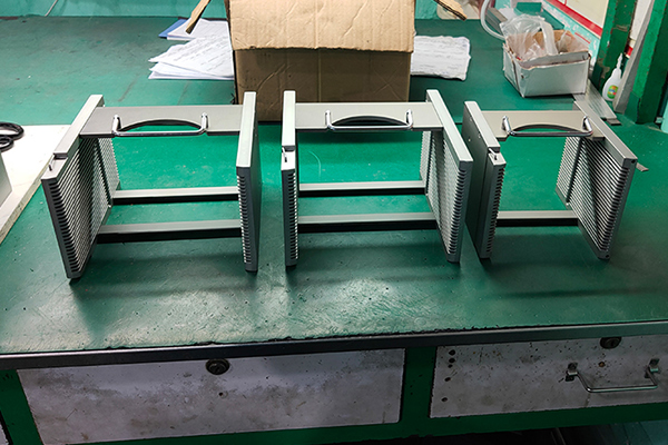
12-inch Metal Wafer Cassette Manufacturer Ensures Stable, Long-Term Supply Without Failures
When many customers look for a supplier of 12-inch Metal Wafer Cassettes, a common concern always lingers in their minds: Can this manufacturer deliver on time?
-
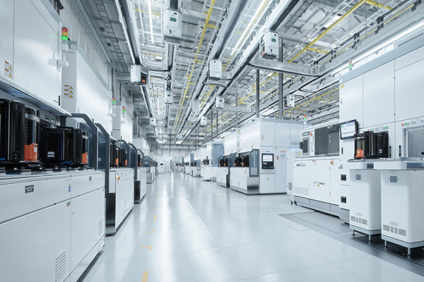
The Future of the Semiconductor Industry: Opportunities and Challenges Coexist
The future of the semiconductor industry is undoubtedly bright. As the cornerstone of modern technology, its development is deeply intertwined with the major trends of global technological innovation.
-
Professional 12-inch Wafer Frame Cassette Manufacturer: Better Understanding Your Customization Needs
With the continuous rise in raw material, labor, and operational costs, reducing expenses and increasing efficiency has become a core challenge for business survival and development.
-
DOHONE Your One-Stop Custom Service Manufacturer for Lead Frame Magazine, Understanding
As various costs continue to rise, businesses are now prioritizing efficiency. More and more customers are seeking one-stop production services—where a single factory handles everything from proposal and design to processing, manufacturing, pre-sales, and after-sales support.
-
Global Artificial Intelligence Transformation
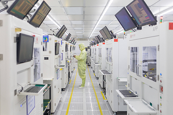
According to authoritative media reports, semiconductor revenue is projected to double from 2024 to 2030, surpassing $1 trillion.
-
An ISO9001 Quality Management System certified manufacturer of 12-Inch Metal Wafer Cassettes
DOHONE — a professional R&D and manufacturing expert in 12-Inch Metal Wafer Cassettes. With a stringent quality control system, we are among the first in the industry to achieve ISO9001 International Quality Management System certification.
-
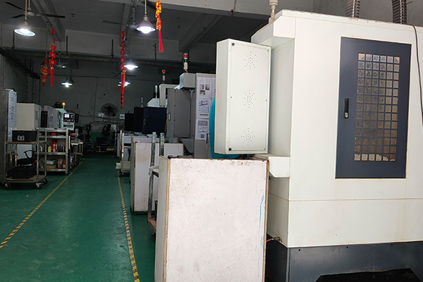
Manufacturer of 12-inch Metal Wafer Cassettes - Creating Value for Customers
At the heart of the semiconductor manufacturing supply chain, the 12-inch Metal Wafer Cassette serves as a critical carrier for wafer transfer and storage.
-
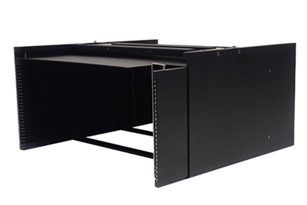
What is the Critical Role of the 12-inch Wafer Frame Cassette in the Dicing Process?
In the precision workflows of semiconductor manufacturing, a 12-inch wafer must be cut into thousands of individual chips, a process known as "dicing."
-
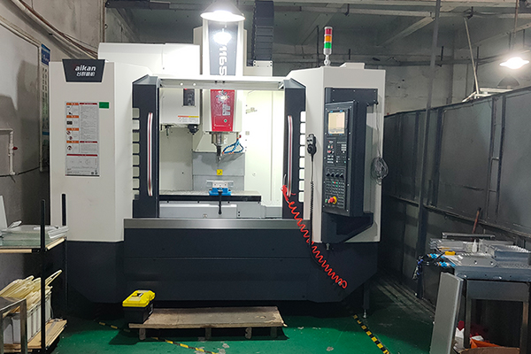
DOHONE Focuses on 12-inch Wafer Frame Cassette
In the semiconductor chip manufacturing industry, wafer packaging, testing, dicing, and storage carriers play a crucial role.
-

DOHONE 12-inch Wafer Frame Cassette
Utilizes a high-precision CNC-machined mushroom head positioning structure with a positioning accuracy of up to ±0.02mm.
-
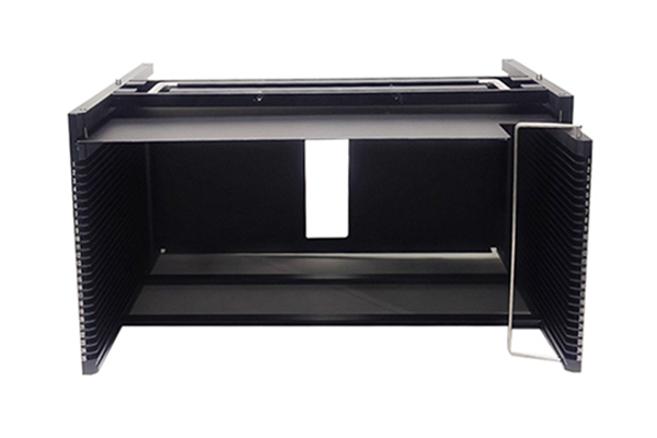
DOHONE 12-inch Wafer Frame Cassette: Dual Assurance for Wafer Processing Quality and Efficiency
The company consistently adheres to a customer-centric approach, providing high-efficiency, high-quality products and services, which has earned the trust and positive feedback from a wide range of clients.
-
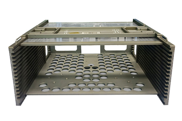
The 12-Inch Wafer Frame Cassette Acts As A "Mobile Fortress" For Wafers
The DOHONE 12-inch Wafer Frame Cassette ensures that wafers remain "unscathed" throughout complex process workflows.
-

DOHONE possesses strong supply capabilities for 12-inch Metal Wafer Cassettes
In the precise processes of semiconductor manufacturing, the safe transportation and storage of bare wafers are directly linked to production yield and cost control.
-

DOHONE Collaborates with Industry Partners to Foster the Sustainable and Healthy Development of the Global Semiconductor Industry
Amid intensifying global technological competition, semiconductors—the core foundation of the digital economy—have become a critical focus in the strategic planning of nations worldwide.
-
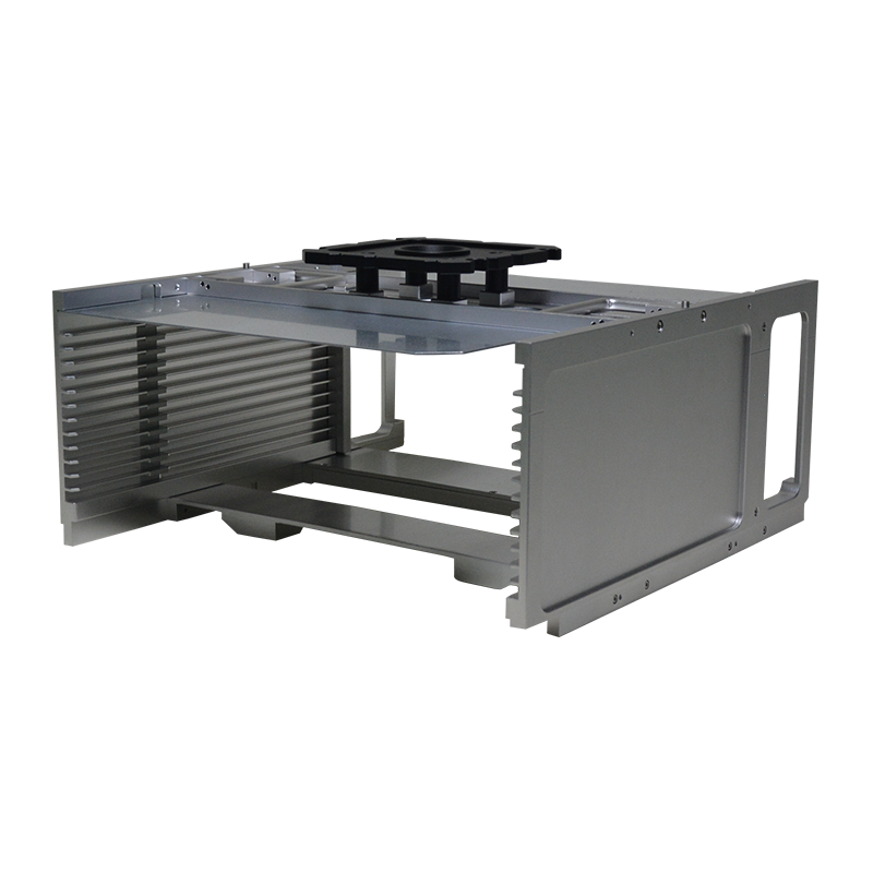
12-Inch Wafer Frame Cassette vs 8-Inch Wafer Frame Cassette: How Size Shapes Performance in Semiconductor Manufacturing
As the semiconductor industry accelerates toward advanced technologies and higher production volumes, the tools used for wafer handling are evolving to meet stricter performance standards. Among these critical tools, the 12-inch wafer frame cassette and 8-inch wafer frame cassette remain the two most widely used formats. Each plays a vital role in supporting wafer thinning, dicing, packaging, and inspection processes, but their differences in size and capacity significantly influence manufacturing efficiency and application suitability.
-
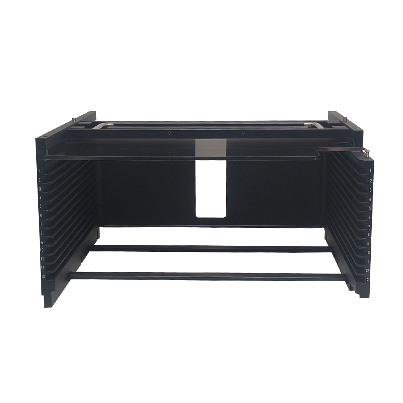
Applications of the 12-Inch Wafer Frame Cassette in Today’s Semiconductor Industry
As semiconductor manufacturing continues pushing toward smaller nodes, higher integration, and faster production cycles, equipment used for wafer handling has become more advanced and specialized. Among these essential tools, the 12-inch wafer frame cassette plays a vital role in supporting precision processing, safe transportation, and clean storage of semiconductor wafers during multiple fabrication stages. Its importance continues to grow as fabs expand capacity for AI chips, 5G components, and cutting-edge logic devices.
-
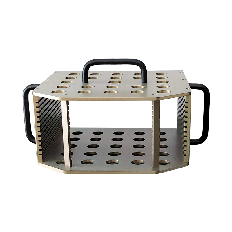
What Is a 12-Inch Metal Wafer Cassette? Understanding Its Growing Importance in Semiconductor Manufacturing
As the global semiconductor industry continues to scale production and push technological boundaries, the demand for high-precision handling equipment is rising. Among these essential tools, the 12-inch metal wafer cassette has become a critical component in ensuring efficiency, safety, and reliability throughout the wafer fabrication process.
-
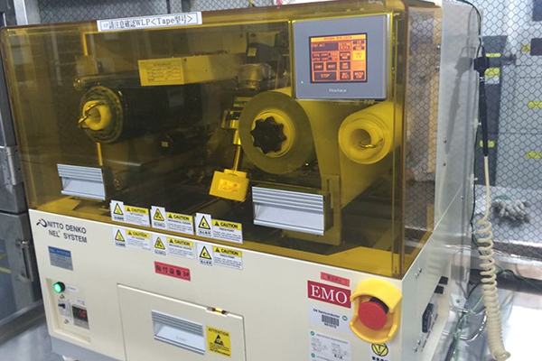
Semiconductor Manufacturing Equipment Market Welcomes Wave of Growth, DOHONE Drives Chip Manufacturing Industry Upgrade
Driven by the accelerated global digital transformation and the iteration of emerging technologies, the semiconductor industry is entering a new golden period of development.
-
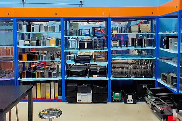
DOHONE 12-Inch Wafer Cassette Helps Customers Enhance Production Efficiency and Product Competitiveness
To meet the demands of different processes and application scenarios, DOHONE has built a comprehensive product matrix covering full-specification wafer cassette products, including 6-inch, 8-inch, and 12-inch.
-
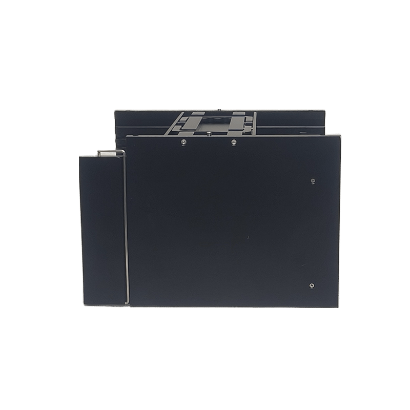
DONG HUNG XIN Recognized as Leading 8-Inch Wafer Frame Cassette Manufacturer
As semiconductor manufacturing continues to advance, high-quality wafer handling solutions have become crucial for protecting delicate wafers throughout production. DONG HUNG XIN, a premier 8-inch wafer frame cassette manufacturer, is gaining recognition for providing durable, precision-engineered cassettes that ensure safe storage, transport, and automated processing in cleanroom environments. With a focus on innovation and reliability, the company is helping fabs worldwide achieve higher yield and efficiency.
-
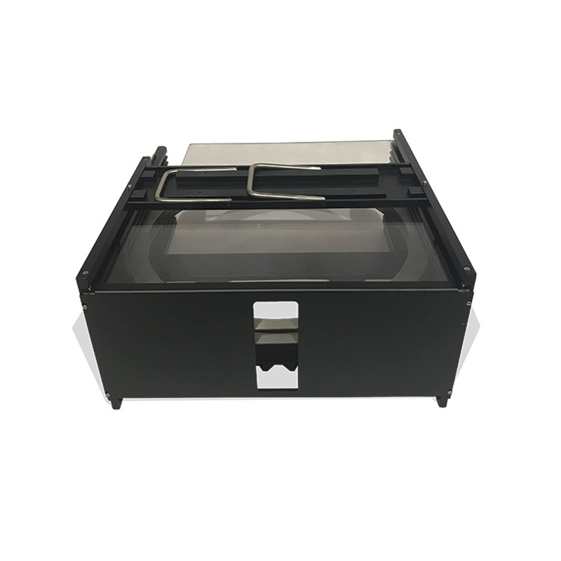
DONG HUNG XIN Leads the Way as a Premier Wafer Frame Cassette Manufacturer
As the semiconductor industry continues to grow, the demand for reliable wafer handling solutions is increasing rapidly. DONG HUNG XIN, a leading wafer frame cassette manufacturer, has gained a strong reputation for producing high-quality, durable, and precision-engineered cassettes that ensure the safe storage, transport, and processing of semiconductor wafers in cleanroom environments. Their commitment to innovation, quality, and customer satisfaction has positioned them as a trusted partner for fabs worldwide.
-
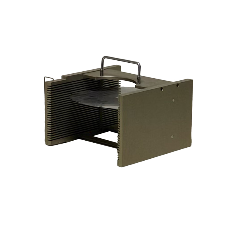
DONG HUNG XIN Emerges as Leading Metal Wafer Cassette Manufacturer for Advanced Semiconductor Industry
As the semiconductor industry continues to expand and evolve, the demand for high-quality wafer handling solutions has never been higher. DONG HUNG XIN, a leading metal wafer cassette manufacturer, is gaining recognition for producing durable, precision-engineered cassettes that support safe storage, transport, and processing of semiconductor wafers in cleanroom environments. With a focus on quality, innovation, and customer satisfaction, the company is setting new standards in wafer handling technology.
-
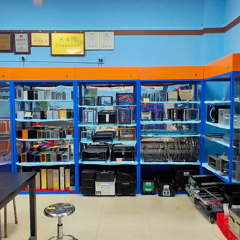
Metal Wafer Cassette: Essential Applications in Modern Semiconductor Manufacturing
As semiconductor manufacturing evolves toward higher precision and larger wafer sizes, the metal wafer cassette has emerged as a vital tool for protecting wafers throughout the production process. Designed for durability, cleanroom compatibility, and precise handling, these cassettes play a crucial role in ensuring product quality, reducing contamination risks, and supporting automated operations in modern fabs.
-
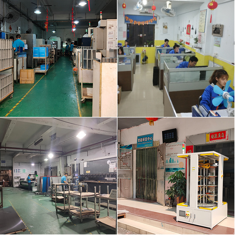
What Is Metal Wafer Cassette
A metal wafer cassette is a specialized storage and transfer container designed to protect semiconductor wafers during manufacturing, inspection, and transportation. As the semiconductor industry continues pushing toward higher precision and cleaner processing environments, metal wafer cassettes have become essential tools for maintaining wafer integrity and ensuring production consistency. Their robust structure, contamination-resistant materials, and compatibility with automated equipment make them a core component in today’s advanced chip-making workflow.
-

Wafer Frame Cassette Finds Expanding Applications Across Semiconductor Manufacturing
As semiconductor production continues to advance at a rapid pace, the Wafer Frame Cassette is becoming increasingly indispensable across multiple stages of wafer processing. Designed to safely hold and transport wafer frames during dicing, inspection, and packaging, this precision-engineered tool plays a crucial role in protecting delicate semiconductor materials and ensuring smooth operation in automated production lines. With the global demand for chips rising, the applications of the Wafer Frame Cassette are expanding in both advanced fabs and specialty semiconductor facilities.
-
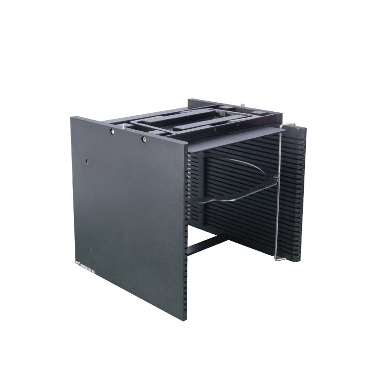
12-Inch Wafer Frame Cassette vs 6-Inch Wafer Frame Cassette: How Size Impacts Efficiency in Semiconductor Manufacturing
As the semiconductor industry pushes toward advanced process nodes and higher production volumes, wafer handling equipment is evolving to meet new demands. Among the most essential tools in wafer processing, the 12-inch Wafer Frame Cassette and 6-inch Wafer Frame Cassette play crucial roles in the safe transport, storage, and automation of wafer frames. With manufacturers navigating increasingly complex production requirements, understanding the differences between these two cassette types has become vital for optimizing efficiency and yield.
-
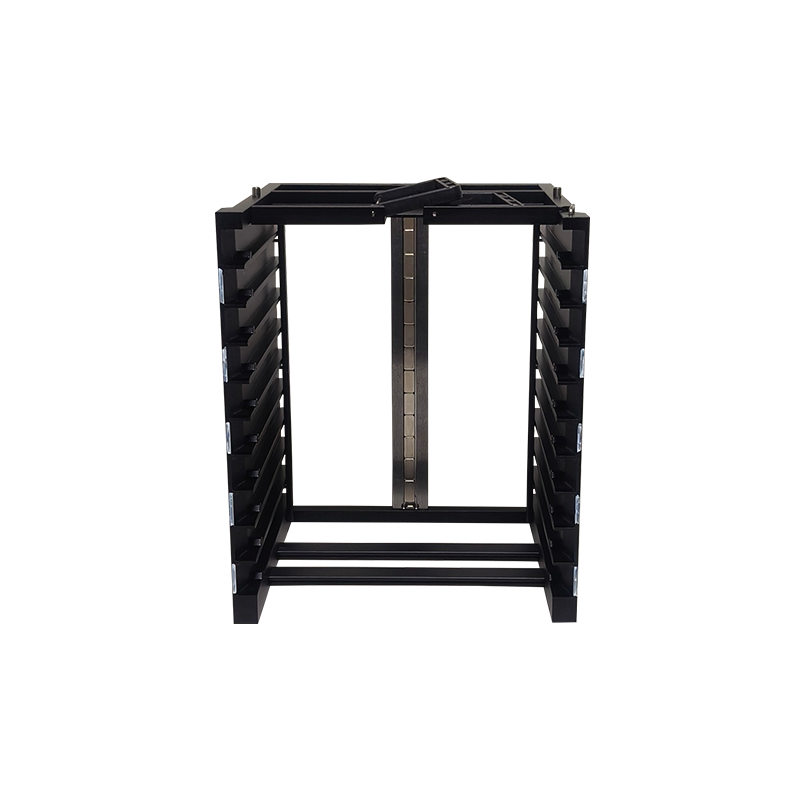
Wafer Frame Cassette Becomes Essential Equipment in Modern Semiconductor Production
As semiconductor manufacturing continues to advance toward smaller nodes and higher precision, the Wafer Frame Cassette has become a critical tool for ensuring safe, efficient, and contamination-free handling of delicate wafer frames. With the global chip industry expanding rapidly, this specialized equipment plays a vital role in supporting high-volume production, improving process stability, and protecting valuable semiconductor materials during transport and storage.
-

Metal Wafer Cassette Processing
The issue was that the Metal Wafer Cassette manufacturer James had partnered with was newly established. Although their equipment was new, they lacked significant experience in processing precision Metal Wafer Cassettes.
-
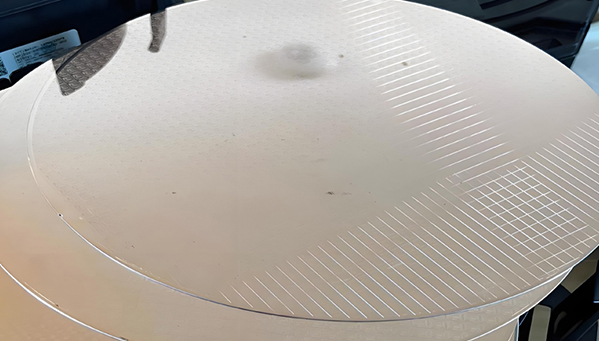
The Deep Interconnection Between Yield and Reliability
In the precise world of semiconductor manufacturing, the wafer serves as the cradle for chips, and the yield and reliability in its production process are like intertwined branches, closely linked.
-
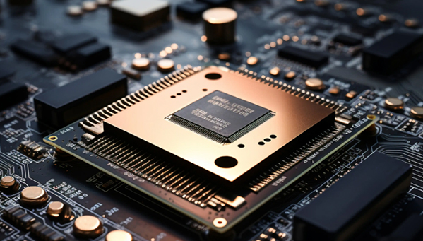
Semiconductor Sales Exceed The Standard
According to an authoritative media report, worldwide semiconductor sales in July 2025 totaled $62.1 billion, up 20.6% from $51.5 billion in July 2024 and a 3.6% increase from $59.9 billion in June 2025.
-
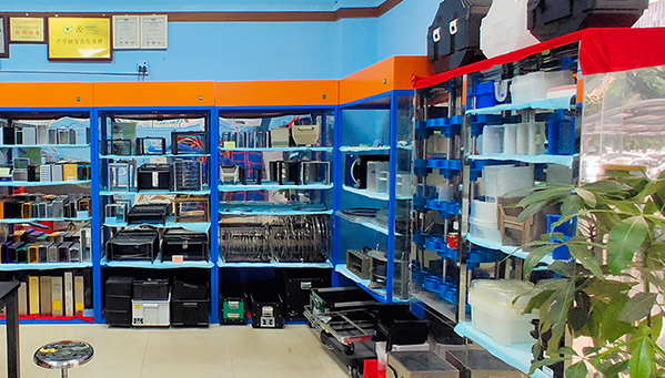
Dedication to Perfecting Every Wafer Cassette is the Mission of DOHONE
As a specialized custom manufacturer of Wafer Cassettes deeply rooted in the core semiconductor support sector, DOHONE consistently integrates the philosophy of "precision engineering and intelligent manufacturing" into the entire product lifecycle.
-

Wafer Ring in Semiconductor Manufacturing
The wafer ring plays a crucial role in the field of semiconductor chip manufacturing. It is primarily used in conjunction with blue tape to secure the wafer onto the film for dicing and scribing processes, providing support, handling, and protection for the wafer.
-
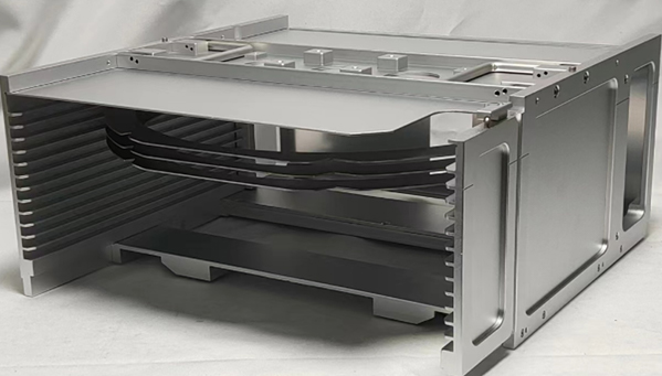
Forecast of the Memory Chip Market Size in 2025
The global semiconductor market is projected to reach $700.874 billion in 2025, with the memory market expected to hit $189 billion, reflecting a growth rate of 13%.
-

Why Is A Wafer Ring Needed To Support The Dicing Tape During Wafer Dicing?
Wafers from the semiconductor foundry require back grinding to reduce their thickness to meet packaging specifications. After grinding, the clean and intact wafer is mounted onto the dicing tape.
-
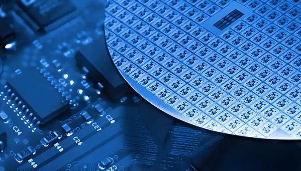
Global Semiconductor Market Size Sees Steady Growth in 2025, with DOHONE Contributing Modestly
According to semiconductor industry data, the global semiconductor market reached $180 billion in the second quarter of 2025, reflecting a 7.8% increase from the first quarter of 2025 and a 19.6% rise compared to the second quarter of 2024.
-
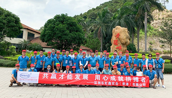
Shenzhen DOHONE Turnover Storage Solutions Team's Qingyuan Two-Day One-Night Adventure Retreat
Shenzhen DOHONE Turnover Storage Solutions has always prioritized enabling employees' dreams and well-being, creating diverse recreational programs for its entire workforce.
-
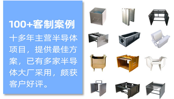
Shenzhen DOHONE's Turnover and Storage Products Strengthen
Shenzhen DOHONE's Turnover and Storage Products Strengthen and Upgrade Industrial Chains towards High-end Applications, Supported by 100+ Enterprise Implementation Cases
-
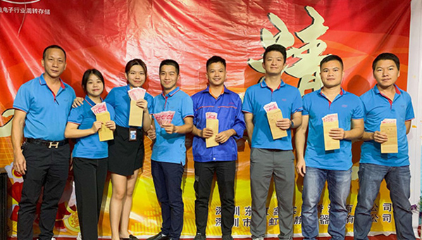
DOHONE Announces Achievement of September Target with Cash Dividend Distribution
Through the concerted efforts of all Donghongxin (DOHONE) family members in September, the company's order volume reached a historic high since its establishment
-
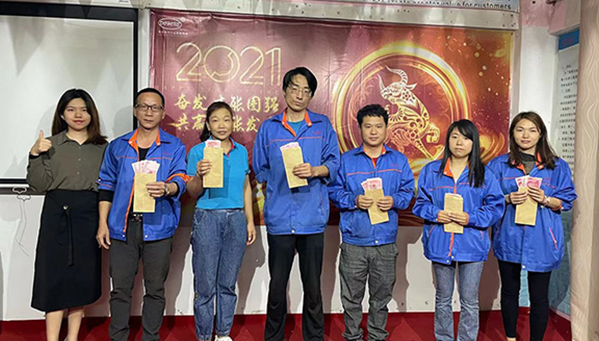
October Recruitment Plan
Established in 2003, we possess an experienced engineering and production team alongside advanced precision machinery, delivering one-stop customized solutions for electronic/semiconductor material handling and storage products.
-
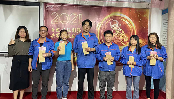
DOHONE Wafer Cassette Factory Celebrates Lantern Festival
The Laba Festival marks the prelude to the Lunar New Year, and the conclusion of the Lantern Festival signifies the end of our celebrations.
-

November Employee of the Month Commendation Meeting
Every Thursday marks the day when DOHONE team members gather for their weekly morning meeting. With bright smiles, all arrived early at the meeting room in preparation.
-
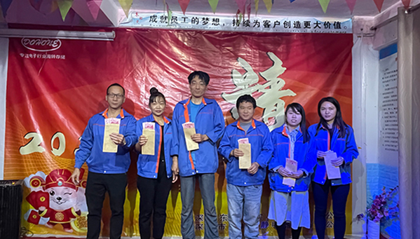
Wafer Cassette Processing Plant Will Disburse November Performance Bonuses
Wafer Cassette Processing Plant will disburse November performance bonuses at the collective all-hands meeting on December 10.
-
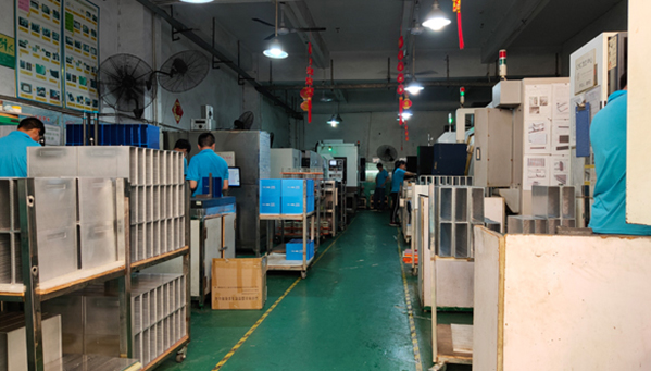
Wafer cassette manufacturer DOHONE wishes you a triumphant Year of the Ox in 2021, filled with auspicious fortune
The year 2020 proved extraordinary as we navigated pandemic disruptions, production resumption challenges, and rising costs of raw materials including aluminum profiles and stainless steel plates.
-
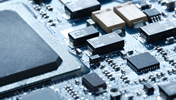
Why Are 12-Inch Wafers So Important
A 12-inch wafer is a circular thin slice made of monocrystalline silicon, serving as the fundamental material for semiconductor manufacturing and the core carrier of integrated circuits.
-
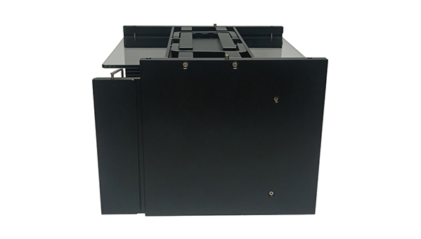
Advantages of DOHONE 8-inch 25-Slot Wafer Frame Cassette
In the back-end process of IC packaging and testing in the semiconductor industry, the 8-inch 25-Slot Wafer Frame Cassette plays a crucial role.
-
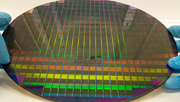
Grand Tech Innovation Sdn Bhd and Dohone's Establish Partnership
Amidst the rapid tide of technological advancement, Grand Tech Innovation Sdn Bhd has emerged as a rising star, swiftly gaining prominence in the field of precision engineering solutions.
-
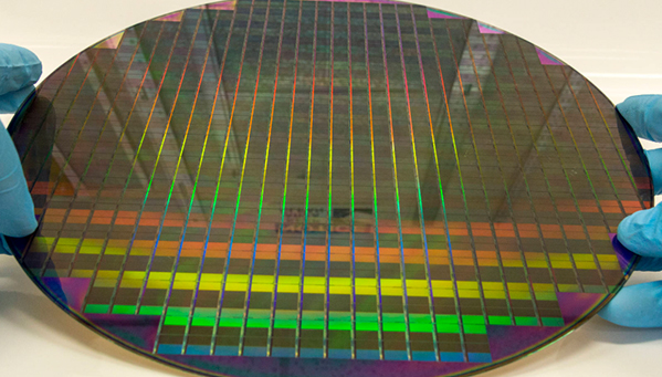
What Are The Main Market Applications Of 8-Inch Wafers
8-inch semiconductor silicon wafers are a critical component of integrated circuits (ICs), such as those used to power computers, mobile phones, and various other electronic devices.
-
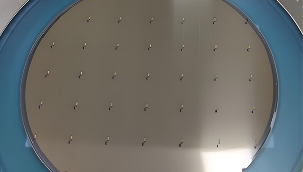
Current Technological Development Status of 6-Inch Wafer Dicing in the Semiconductor Chip Manufacturing Industry
In the semiconductor chip manufacturing sector, wafer dicing is a critical process that separates numerous chips on a wafer into individual units.
-
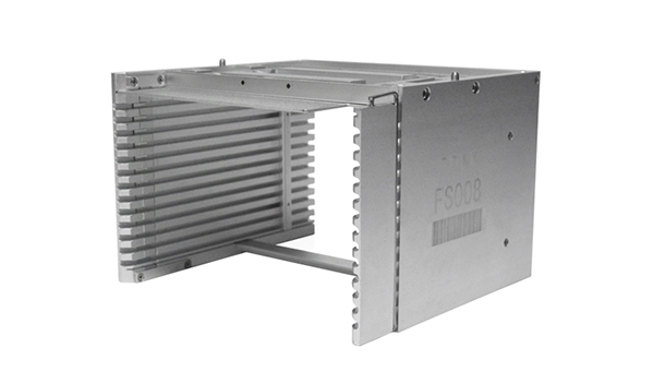
DOHONE 6-Inch 13-Slot Wafer Frame Cassette Revolutionizing Wafer Transfer Experience
In the precision-driven field of semiconductor manufacturing, the DOHONE 6-Inch 13-Slot Wafer Frame Cassette stands out as an efficient solution for wafer transfer with its groundbreaking auto-locking design.
-
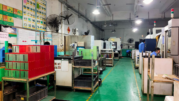
Which Wafer Frame Cassette Factory Is Truly Reliable And Suitable For Long-Term Cooperation?
Wafer Frame Cassette has become an indispensable carrier in semiconductor chip packaging and testing processes, serving as one of the essential accessories for wafer dicing machines.
-
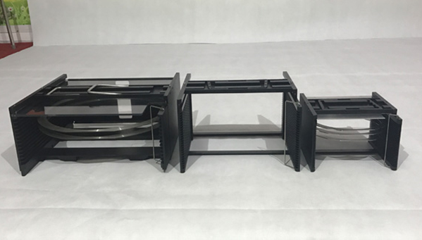
DOHONE company releases another batch of Wafer Frame Cassettes.
Good news alert: Congratulations to DOHONE for producing another large batch of Wafer Frame Cassettes! This order comes from a renowned precision laser equipment manufacturer in Shenzhen.
-
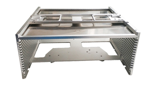
Tay Tool Engineering Works establishes a strategic partnership with Dohone's.
Tay Tool Engineering Works develops and manufactures components for various industries and mechanical equipment.
-
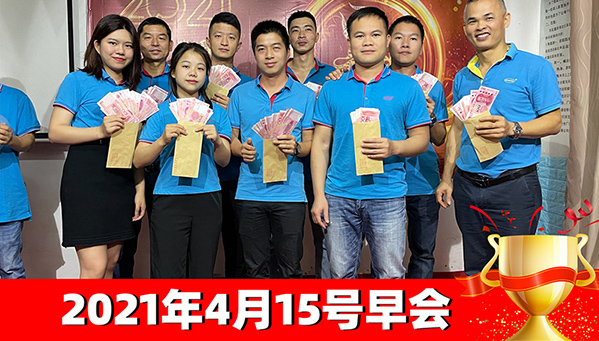
DOHONE March Target Achievement Awards Ceremony
Since the beginning of 2021, DOHONE has been operating at full capacity with a steady stream of orders. Through the collective efforts of all employees in March, the company successfully achieved its monthly shipping targets.
-
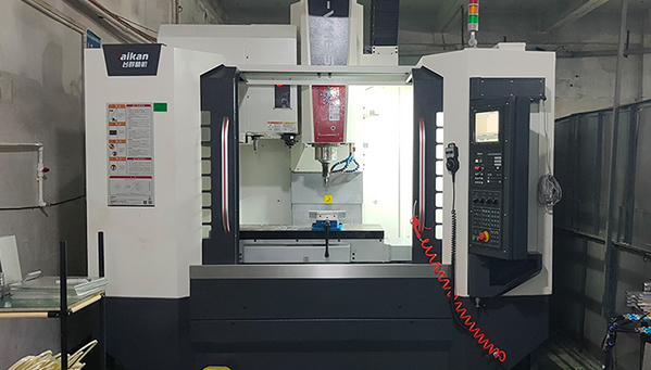
Wafer Cassette Manufacturer Deploys Long-Stroke Precision Machining Systems
Wafer cassette manufacturer deploys long-stroke precision machining systems, enabling faster batch customization and accelerated delivery.
-
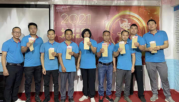
DOHON April Target Achievement Awards Ceremony
The most anticipated moment of the month has arrived again. Through the collective efforts of all Donghongxin employees in April, we successfully achieved our monthly targets.
-
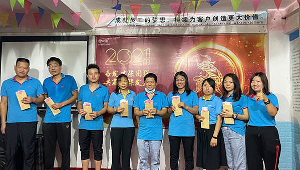
Dohone Achieves May Performance Targets - Employee Bonus Distribution
May brings rising temperatures, yet this fails to dampen the dedication of Dohone’s workforce. Every employee dedicates themselves fully to their responsibilities – collective commitment drives our corporate targets.
-
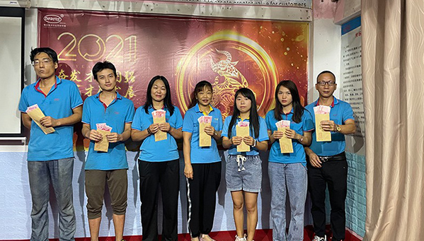
On-Site Presentation of June Target Achievement Awards
The first half of 2021 has passed imperceptibly. The semiconductor industry demonstrates strong market performance amid growing support from the Chinese government.
-
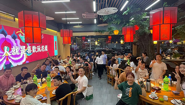
DO·HONE Semiconductor Mid-Autumn Festival Celebration
Inspired by the timeless poetic verse "May we all be blessed with longevity though separated by thousands of miles, sharing the beauty of this moon together,"
-
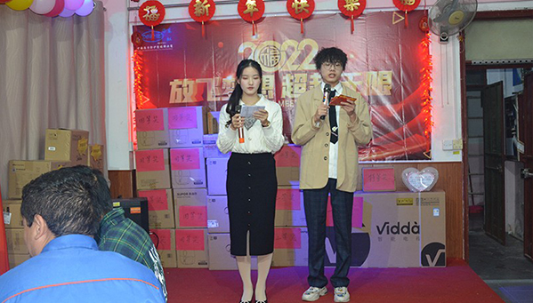
"Unleashing Dreams, Transcending Boundaries" – DO·HONE Annual Gala
As time swiftly passes, 2021 has drawn to a close while 2022 approaches with renewed hope and promise. The new year brings fresh objectives and aspirations.
-
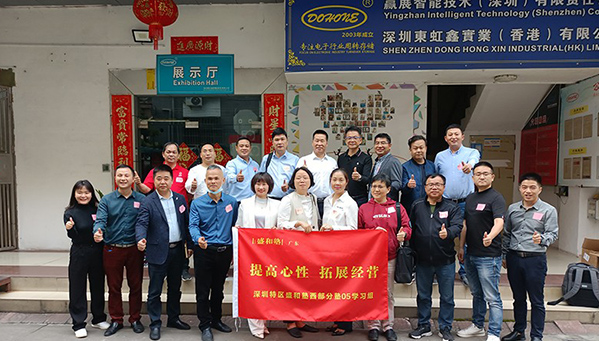
Shenzhen Seiwa Jyuku Successfully Holds Western Branch April Study Session at DO·HONE
Amid April's vibrant renewal, the Western Branch 05 Study Group of Shenzhen Seiwa Jyuku convened its latest knowledge-sharing session at DO·HONE Static Control Equipment/Yingzhan Intelligent Technology's facilities.
-
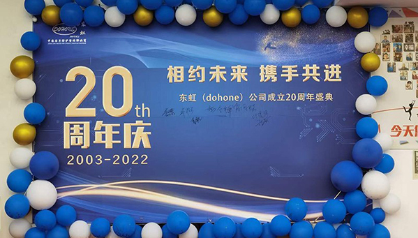
DO·HONE 20th Anniversary Celebration
Twenty years have passed in the blink of an eye - a period sufficient to witness a corporation's remarkable growth and achievements, as well as the formation and evolution of an exceptional team.
-
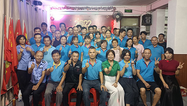
Mid-Autumn Festival Celebration at China's Premier Semiconductor Protection Solutions Provider
The Mid-Autumn Festival is an important occasion for family reunions, yet many working professionals across industries are unable to return home due to various commitments.
-
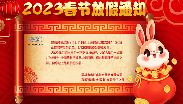
DOHONE 2023 Official Holiday Schedule Notice
The year 2022 has been an extraordinary journey of challenges and triumphs. We extend our deepest gratitude to all partners.
-
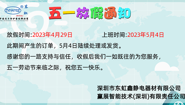
DOHONE - Semiconductor Protection Solutions Provider: Labor Day Holiday Notice
As the 2023 Labor Day approaches, DOHONE - your trusted semiconductor protection solutions provider - will observe a 5-day holiday from April 29 to May 3. Normal operations will resume on May 4.
-

DOHONE Wishes You a Joyous Mid-Autumn Festival & National Day Celebration
At this special occasion marking both the Mid-Autumn Festival and China's National Day, all DOHONE employees gather together in celebration of these two culturally significant holidays.
-

DOHONE Team Building Retreat: A Two-Day, One-Night Journey of Collaboration and Growth
DOHONE successfully conducted a two-day team-building retreat on July 7-8 at Shantou's Nan'ao Island and Chaozhou Ancient City, renowned scenic spots in the Chaoshan region.
-
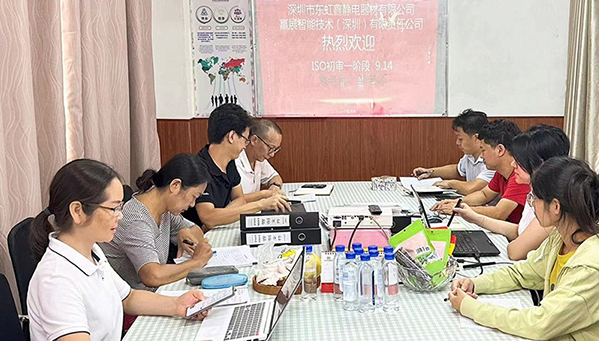
Dohone Certified with ISO 9001:2015 QMS, Advancing Premium Service Excellence
From raw material procurement to every step of production, and finally to product inspection and delivery, it provides clear standards and protocols.
-
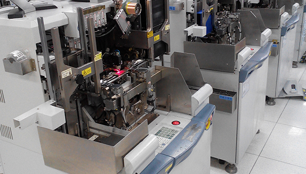
Insights into Emerging Demands for Chip Packaging and Testing: Embarking on a New Journey for the Semiconductor Industry
In the current era of surging digitalization, the semiconductor industry, as the core driving force of technological development, continues to demonstrate astonishing vitality and transformative power.
-
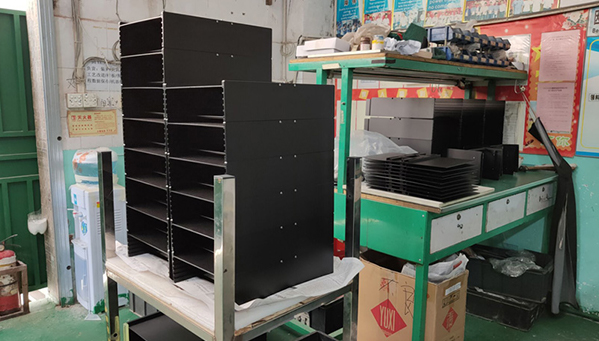
Insight into the Global Development Status of Wafer cassette
In the vast ecosystem of the semiconductor industry, the wafer carrier, as a crucial tool ensuring the safe and efficient flow of wafers during production, transportation, and storage, is closely related to the overall trend of the semiconductor industry.
-
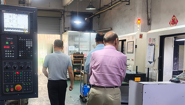
Donghongxin Welcomes Indian Clients for Facility Tour, Exploring New Collaborative Opportunities
Recently, Donghongxin hosted a delegation of key clients from India, who traveled thousands of miles to visit our headquarters for an in-depth facility inspection.
-
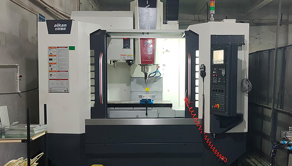
Donghongxin Adds Precision Processing Equipment for Wafer Cassettes
In the semiconductor wafer cassette manufacturing industry, every technological advancement and equipment upgrade resembles a critical sprint in a race, determining whether a company can maintain its leading position.
-
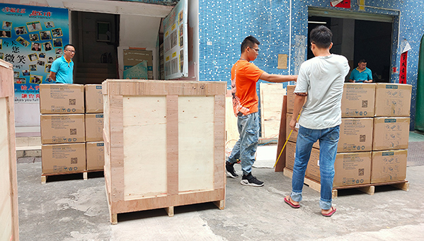
Donghongxin Semiconductor Carriers Depart for Morocco, Embarking on a New Chapter of Global Collaboration
Amid thriving global trade, Donghongxin Semiconductor has taken another decisive step forward, leveraging our exceptional quality and efficient production capabilities!